The workbench
One flow, from cell to packaged chip
The workbench holds the whole design: a per-domain workspace, a solver cockpit, and an evidence trail recording what produced what. Pick a stage, run it, decide from the results.
Platform flow
The stages, and what runs at each one
Every stage is a recorded job, not a script you hope behaves. Pick one.
Candidate compare
Choosing, with the evidence in front of you
Every stage ends in a decision. Candidates are compared against the target, and the one that is picked carries its evidence.
Target
Platform
Band
Illustration with sample data — no design is running here. Open the platform to generate real candidates, and to see which checks each one passes.
The tile
Five domains, one package
A cross-section of the co-packaged optics tile: carrier PCB, EIC driver die, flip-chip bumps, PIC ring crossbar, and lensed fiber array — designed together in one browser workspace.
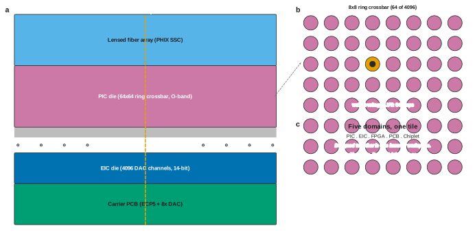
Publication-quality vector figure generated with the schematic-figure skill (MIT, lgwrightlab). Full design process: figure/docs/brief.md, spec.md, facts.md, concepts.md.
From spec to signoff
Verified outputs, not just simulations
A layout that simulates is not a layout that can be built. Every stage has to survive a check that is capable of failing it.
Three outcomes, not two. A verification run ends CLEAR when every applicable mode was verified, NEEDS GUARDS when there are silent gaps, and BASELINE FAILED when the design does not even simulate. Reporting the gaps is the point.
AI proposes. Deterministic engines dispose. Designers decide. The platform is built so that the last of those three is always a person. Meet the agents →
Where the cost actually is
Finding out why it failed
“Does it pass?” is the easy half. Wilson Research puts debugging at 44–47% of project time, so we ship the toolchain that ends in a cause, not a guess.
What is measured, and what is quoted. The fault-injection suite, the diagnosis classifier, the waveform queries, the formal anchors, the relation graph and the gate list are all in the platform and run today. The 44–47% figure is third-party — Wilson Research, cited in our own reference notes via artl.ai — not a measurement of ours.
Reliability & qualification
JESD264, clause by clause
JEDEC's silicon-photonics qualification framework is executable here: every clause mapped to its test conditions, sample sizes, intervals and pass-fail criteria, then reported clause by clause.
Every clause, what it covers and what it applies to24 clauses
| Clause | What it covers | Applies to |
|---|---|---|
| 4.2 | Reliability and service-life requirements | All SiPh products |
| 4.3 | Standard production screening | Qualification dies and sub-components |
| 4.4 | Sample selection and test vehicle | All qualification samples |
| 4.6 | Measurement intervals | All stress-based tests |
| 4.7 | ESD characterization | Bare dies and integrated chipset assemblies |
| 5.1 | Generic micro-optic devices — the base stress matrix | Modulators, PDs, waveguides, thermal resistors |
| 5.2 | Photodiode qualification — dark current, responsivity, SOA, TDDB, high optical power, HCI | Photodiodes |
| 5.3 | Electro-optic modulator qualification | PN, PiN, SISCAP, EAM |
| 5.4 | Thermo-optic phase-shifter qualification | TOPS, resistor element in BEOL |
| 5.5 | Thermal resistor qualification | FEOL silicon |
| 5.6 | Decoupling capacitor qualification | FEOL polysilicon or SiOx |
| 5.7 | Waveguides and passive optics | Splitters, couplers, PSR, MUX/DMUX, VOA, crossings |
| 6 | Bare die — no optical or active devices attached | SiPh die |
| 7 | Integrated chipset, with or without flip-chip attached die | 1D–3D integration |
| 8.1 | Die pad wirebonding — pull and ball shear | DRIE cavities / UBM processed outside the foundry |
| 8.2 | Component shear | Directly attached die, chips and optical sub-devices |
| 9 | BEOL reliability — Al, Cu, W, contacts, vias, MIMCAP, resistors | Back-end structures |
| 10 | TSV / chip-on-chip / chip-on-chip-on-substrate stack-up | All 2.5D and 3D stacking |
| 11.1 | Laser on submount, and butt-coupled lasers | Fabricated lasers adjacent to the die |
| 11.2 | Fabricated laser attached to the SiPh die | Solder, metal or polymer bond |
| 11.3 | Laser chiplet bonded to the die surface, and micro-transfer printing | III-V, TFLN and LN coupons |
| 11.4 | III-V laser grown epitaxially in the SiPh wafer | Under investigation, not commercialised |
| 12 | Optical I/O — fibre array unit attach | Edge, vertical and evanescent coupling |
| 13 | Manufacturing process, QC, yield, data, traceability and ORT | Wafer fab and assembly |
Clause 11 matters most for photonics: laser integration is four distinct qualification problems, because a laser on a submount, bonded to the die, micro-transfer-printed and epitaxially grown do not fail the same way.
Twenty-four clauses, eighty-two protocols. The six that stress a part and measure it are executable, not prose: each computes its own pass or fail against the standard's end-of-life criteria and extrapolates a lifetime.
Depth
Three things most flows do not do
Each of these is a place where the industry settles for an estimate. We measured instead, and the measurement is what the claim rests on.
Where these stand. All three are implemented and measured on our own reference cases, which is what the figures above report. They are not claims about every process or every design — a clearance check is only as good as the solids it is given, and the derivative check only as good as the deck it reads.
Proof
What we have actually done
Not a roadmap. Each row is something that exists, and where the platform has a number for it, the number is here.
| What we have done | What it means |
|---|---|
| Design-rule clean chip layouts | Our designs pass foundry signoff checks and are ready for fabrication |
| Photonic compute precision on real models | 27.4 dB signal-to-noise on GPT-2 Small and 27.5 dB on GPT-2 Medium, at full precision |
| SPICE-verified analogue cells | Circuit performance confirmed in simulation before anything is fabricated |
| Full-stack chip integration | Photonic, electronic, firmware and packaging designed together in one platform |
| Calibrated on measured data | Models trained on measurements from real components, not only on simulation |
| Machine-checked temporal proofs | Control RTL proven for safety and liveness — with reachability covers, so no proof passes vacuously |
| Second-source-ready parts | Component groups verified for footprint and pinout compatibility across manufacturers |
| Packaging clearances measured, not assumed | Solid geometry returns interference volumes with keep-out limits, and the closed-form and kernel paths agree to within 2×10⁻⁶ % |
| Analogue validated beyond DC | Device behaviour confirmed across simulation formulations, plus noise-path validation |
| A live design platform | A working web IDE with agents, design tools and verification, reachable from anywhere |
- 5 → 1
- PIC, EIC, FPGA, PCB and Chiplet in one project tree
- 6
- PDKs with an explicit DRC support status — including the limited ones
- 3
- Measurement platforms feeding the model calibration
- 0
- Signoffs taken on an AI's word alone
Read this before you commit a run
Know the limits first
Support differs by process. This is the honest picture of our DRC signoff path per PDK, taken from our own support matrix.
| Platform | Type | DRC path in the IDE | Status |
|---|---|---|---|
| IHP SG13G2 | SiGe BiCMOS | Layout-native checker + independent second engine | Full |
| SG13CMOS5L | CMOS | Layout-native checker + second engine | Near-full |
| GF180MCU-D | CMOS 180 nm | Layout-native checker + second engine | Near-full |
| GF180MCU-A | CMOS 180 nm | Independent second engine only | DRC-only |
| IC Sprout 55 | CMOS 55 nm | Independent second engine only | DRC-only |
| SKY130A | CMOS 130 nm | Layout import path | Layout import |
| CORNERSTONE SOI | Silicon photonics | Photonic cells, DRC and EM solvers | Photonic flow |
What the statuses mean. Full — both the layout-native checker and the independent second engine are available. Near-full — both run, with known rule-coverage gaps we can name. DRC-only — only the independent engine is wired up, so we do not claim parity with the layout-native path. Layout import — layouts can be read and edited, but treat DRC as your responsibility in that process. Ask us for the current matrix before you plan a tapeout.
Devices & foundries
What you can design today
Photonic and electronic design in one catalogue — cells, waveguides, splitters, couplers, crossings, modulators, detectors, heaters, pads, die templates — each with the ports, cross-sections and measured S-parameters it needs to be simulated.
| Platform | Material system | Used for |
|---|---|---|
| SOI 220 nm | Silicon-on-insulator | Waveguides, rings, MZIs, grating couplers |
| SOI 340 nm | Silicon-on-insulator | Waveguides, rings, MZIs |
| SiN 300 nm | Silicon nitride | Low-loss passives, visible / near-IR |
Component counts, layer maps and port lists are read live from the platform catalogue, so they change as PDKs are imported. Ask for the current numbers rather than quoting these names as a fixed list.
IP, exports & deployment
Your designs never stop being yours
Built for teams whose layouts cannot leave their control: you own what you make, you can verify it independently, and you decide where it runs.
Where the work runs
Deployment options are engagements, not a button on a pricing page. Tell us the constraint — data residency, air-gap, procurement — and we will tell you honestly whether we can meet it today.
Don't take our word for it
Verify our work yourself
Every design leaves in formats your bench already reads. Re-run the simulation and compare — if they disagree, that is a bug we want to hear about.